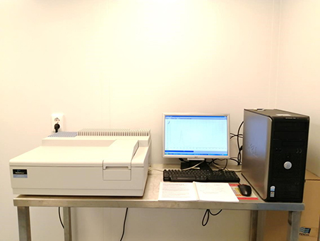
5.1. JEOL JSM-IT700HR / LA
The scanning electron microscope, equipped with an energy-dispersive X-ray spectrometer (EDS), is capable to examine a wide variety of samples and determine their elemental composition. With the help of the thermal field emission (Schottky) electron source, high-resolution images can be taken, so the device is also suitable for examining samples in the nano-size range. The low vacuum mode also allows direct examination of non-electrically conductive samples.
The main features of the device:
Field Emission Electron Source (FE)
Acceleration voltage: can be changed arbitrarily between 0.5 and 30 kV
Resolution: 1.0 nm (high vacuum, SE detector)
Magnification 5x – 300 000x
Possibility to test electrically non-conductive samples in low vacuum mode (10 – 150 Pa)
Possibility to test large samples; maximum sample size: 200 mm (Ø) x 75 mm (height)
Detectors:
Secondary electron (SE) detector
Secondary electron (SE) detector optimized for low vacuum mode
Backscattering electron (BSE) detector
Energy dispersive X-ray spectrometer (EDS) for elemental composition analysis (30 mm2 active surface; 128 eV energy resolution; detection of elements from beryllium to uranium)
Possibility of image and element map montage from a larger sample area
More information: https://www.jeol.co.jp/en/products/detail/JSM-IT700HR.html
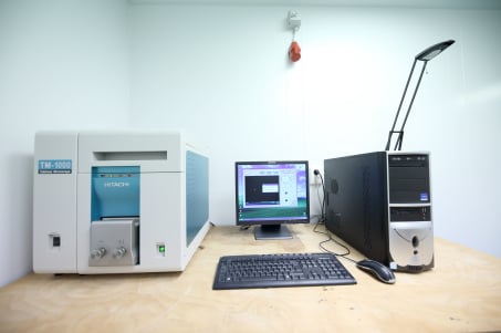
5.2. Hitachi TM-1000 desktop device
The main features of the device:
Tungsten cathode
Compact size (513 x 478 x 564 mm)
Magnification 20x – 10,000x
Acceleration voltage: 15 kV
Maximum sample diameter: 70 mm
Maximum sample height: 20 mm
Backscattering electron (BSE) detector